
Over the past 10 years, the cellular industry has seen dramatic changes in both the requirements on, and the capabilities of the radio to support the wireless connection. The radio has evolved from a single-mode, triple-band 2G system in year 2000, to a triple-mode, 9-band (4×GSM, 5×UMTS with HSPA+), high-speed data-capable system in year 2010. And this new capability required only a third of the physical area. This evolution was driven by both: CMOS technology evolving from 0.35 µm to 65 nm, and smart integration in the front end including product innovations such as converged PAs and highly complex antenna switch modules together with more capable and compact filters.
The trend continues today with rapid deployment of 4G LTE systems, driving new bands and modes of operation. While the CMOS may continue to scale, the analog signal-conditioning RF front end and antennas pose particular challenges to scaling due to physical limits. For the front end to be able to support the continuing evolution, new enabling technologies must be introduced as we approach the limits of improvements through packaging and hybrid integration. Antenna bandwidths are highly constrained by the physical volume requirements. Tunable RF components will enable the continuation of the market requirement for significant reduction in size and total volume as the number of bands and modes increases. Additionally, tunability enables handset form-factors previously only realizable in single-mode applications, allowing for example a single antenna to cover all traditional cellular bands as well as new LTE bands.
Today, several technologies offer a useful tunable RF capability. Traditional technologies such as switched capacitor networks (RF switch plus integrated MIM capacitor), as well as newer technologies such as Barium Strontium Titanate (BST) and Micro Electro-Mechanical Systems (MEMS) are all now in use. These approaches all offer the ability to dynamically change the impedances within a RF component while introducing a minimum amount of loss. The ability of these various technologies to meet the new requirements of the rapidly-expanding RF front end is examined in detail herein.
Since the digital cellular revolution began in the early 1990s, operators and handset manufacturers alike have been striving to increase the functionality of the handset. User demands have moved from simple voice communications, to roaming across different networks, perhaps on different frequency bands, and eventually to higher data bandwidths to support highly capable smartphones and other mobile computing devices.
For example, initial 2G GPRS systems could transmit data at a rate of 56 kb/s (using four time slots), while 2.5G EDGE systems increased that rate to 384 kb/s. Devices with 3G capability could achieve data rates as high as 2 Mb/s, though achieving these high speeds became more dependent upon the user environment. This trend continues with 4G, where the expected theoretical data rates are as high as 70 Mb/s. The higher data rates drive the need for additional spectrum, expanding from single-band operation in the early 1990s to over 38 bands supporting 2/3/4G worldwide bands from 700 to 3500 MHz and continuing to expand. At the same time, the mobile device itself is driving toward more compelling form-factors, with tradeoffs between screen size and overall bulk, leading to extremely thin designs. This “Thin is In” trend reduces the effective bandwidth capability of the antenna, especially at low frequencies. Thus handsets that cover both voice-capable bands, such as Band V or Band VIII as well as a low-frequency LTE band such as Band XII or XIII, have been driven to use multiple antennas.
An interesting industry observation by Jan-Erik Mueller of Intel Mobile Communications captures this trend. In the past decade, we have seen the radio evolve from a single-mode, triple-band 2G system to a tri-mode, 9-band (4×GSM, 5×UMTS with HSPA+) system utilizing only a third of the physical area, and expectations are that this trend will continue. This has been coined “Mueller’s Law,” applying to the cellular radio as Moore’s Law applies to integrated circuits.
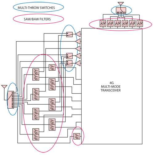
Figure 1 Wireless front end complexity and challenges to scaling.
While the digital portions of the radio continue to scale following Moore’s law, the analog front end elements (filters, switches, amplifiers, antennas) have depended mostly on improved packaging and integration to support the trend while the core functional elements do not scale due to physical power and frequency limitations (see Figure 1). Thus either additional elements must be included to cover the additional bands/modes or the elements must have sufficient bandwidth to cover all or groups of modes which limits their size and performance.
Tunable RF technology is changing the game. In recent years, tunable RF technologies have allowed the front end designer more freedom to create configurable matching circuits. These can be used to adjust the antenna match to reduce mismatch loss and improve the overall efficiency of the antenna at frequencies other than the original design frequency, enabling a single antenna to be utilized for more modes. Tunable RF circuits can also be used for antenna load tuning, where the tunable capacitor is inserted at the antenna load (ground) to change the effective electrical length of the antenna. This was initially implemented using discrete switches and capacitors, but now can be accomplished with higher precision, multiple tuning states and lower losses. Also, these tuning elements enable a new generation of compact tunable filters along with tunable RF matching for power amplifiers and LNAs. In addition to improving the scaling of the RF front end, the availability of high Q and highly linear tunable capacitors leads to improved system performance in compact form factors and can also enable entirely new front end architectures.

Figure 2 Traditional load switch.
Technologies
Three basic technologies are currently being utilized for tunable RF, primarily focused on antenna tuning at this time. These technologies are:
Switched Capacitors
Field Effect Transistors (FET)have been used for several years to provide antenna load tuning.1 This load-tuning approach typically used a SPDT switch to choose between two different discrete reactive networks (capacitive or inductive) to modify the resonant frequency of the antenna (see Figure 2).
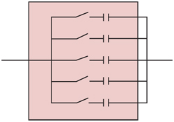
Figure 3 Switched capacitor.
Switched capacitor solutions today utilize either GaAs or CMOS switching FETs with integrated metal-insulator-metal (MIM) capacitors, typically in a 4- to 6-bit configuration (see Figure 3).
FETs have an inherent tradeoff between on-resistance and off-capacitance, which can be characterized by an industry-standard figure-of-merit, Ron·Coff. The on resistance affects the Q of the device, while the off capacitance increases the parasitic loading due to the off branches. For reasonable performance, FETs fabricated using either GaAs j-PHEMT, silicon-on-sapphire (SOS), or silicon-on-insulator (SOI) with gate lengths in the 0.13 to 0.25 µm are integrated with MIM capacitors. For high power applications, voltages as high as 40 to 100 V are encountered due to the high VSWR encountered in antennas. In many cases, the breakdown voltage of the transistors and/or capacitors will not meet the power handling requirements and must be stacked, increasing the insertion loss and cost/size accordingly.
SOS or SOI FETs approach pHEMT devices’ Ron, in the range of 1.5 to 2.5Ω mm. These technologies have similar off capacitances leading to Ron·Coff figure-of-merit of 200 to 400 femtoseconds. For an overall capacitance ratio of 5:1 together with associated MIM capacitor losses and parasitics, this leads to an effective Q in the maximum capacitance state at 1 GHz of 25 to 50. For impedance matching applications, and for antennas with relatively low VSWR, this moderate Q for the switched capacitor solution may yield acceptable performance. The silicon FETs operate from standard control voltage levels, so no additional voltage levels need to be generated for operation. The digital interface can be integrated directly onto silicon switched capacitors but a separate CMOS controller is required for GaAs circuits.
Advantages:
- Low voltage operation
- Total switching cycles
- Low parasitic shunt capacitance
- Low cost, high volume, standard technology
Disadvantages:
- Low Q and/or low ratio (tradeoff)
- Low breakdown voltage
- Linearity (IP3, harmonics)
Barium Strontium Titanate (BST)
Ferroelectric and paraelectric materials provide controllable and high capacitance density utilizing their high dielectric constant which can be varied with applied voltage. BST is the most common paraelectric for RF application which exhibits about a 3:1 capacitance variation with applied voltage where the ratio is intentionally limited to provide stable temperature operation and reasonable linearity.
Figure 4 Single BST capacitor.
When the applied electric field is near zero, the unit cells in the crystal lattice are easily polarized leading to the peak dielectric constant and thus to a large capacitance value when used as a capacitor dielectric. As an electric field is applied, the resulting polarization reduces the sensitivity to additional field which lowers the effective dielectric constant. This inherently nonlinear behavior is used to build variable capacitors that are controlled by the applied voltage. Lower losses are possible than those available from switch-based systems leading to an expanded range of applications. However, the basic thermodynamics of the operation can lead to thermal stability issues. Substantial investments in improved materials and circuit operation points have mostly addressed these issues. Note that the analog control requires high voltages. The high voltage control is implemented in a separate chip that also includes a serial interface. The key limitations currently include low tuning ratio, marginal linearity and cost of the hybrid analog system.
BST capacitor fabrication is not yet compatible with monolithic CMOS integration thus requiring a separate control chip for use in a handset. This chip would provide a programmable charge pump to generate the variable high voltage and may also include an integrated digital interface and other circuitry. Note that this is a smoothly varying analog capacitor as compared to the inherently digital nature of the switched capacitors.
As BST provides a single variable capacitor without the need for a FET switch in series with the capacitor, the overall Q of this approach is higher (see Figure 4). As the voltage is applied across the same terminals as the RF, special consideration must be taken to maintain linearity so the RF or low frequency modulation does not directly modulate the capacitance which would add spurious content. This involves stacking the capacitors to reduce the RF voltage across individual capacitors and alternating the polarity of the DC control voltage to improve linearity. However, stacking the capacitors directly reduces the effective capacitance density.
Advantages:
- Moderate Q
- Total switching cycles
- High capacitance density feasible
Disadvantages:
- Linearity
- Tuning ratio
- Analog control, requires control chip
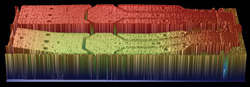
Figure 5 MEMS capacitor elements top element "off," lower element "on."
Micro Electro-Mechanical Systems (MEMS)
MEMS technology is now available for RF applications.2 This technology consists of CMOS-integrated movable mechanical structures which provide the tunable capacitance. The small mechanical beam is actuated with electrostatic force applied through an integrated CMOS controller with the beam directly part of the RF network. Thus, the RF path for each MEMS beam is essentially a pair of metal traces with either a capacitor dielectric (“on” state) or air gap (“off” state) separating the two metal traces (see Figure 5). These MEMS beams are configured into an array to form a digital capacitor with many states (equivalent of 6- to 9-bits of resolution). The array can be sub-divided into series and/or shunt branches, or some combination.
MEMS provides performance enhancements to many of the afore-mentioned deficiencies. The RF path is through metal traces on a mechanical device (with virtually no frequency response at RF) rather than a solid-state junction, so the Q and linearity are much higher. Also, for the commercially available MEMS products, the DC voltage is physically separate from the RF path; thus, the voltage handling is quite high at well over 120 V peak. Traditionally, MEMS devices have required specialized packaging to maintain the hermetic environment around the movable structures, but the technology now allows for fully encapsulated devices at the wafer level and enables standard low-cost packaging or even wafer level chip scale packaging. As a mechanical device, however, there exists an aging effect which eventually will cause device failure, related to wearout. MEMS devices are digital devices exhibiting very little temperature dependence, with temperature coefficient of capacitance in the sub -200 ppm/°C range.
Advantages:
- High Q
- High linearity (IP3 and harmonics)
- Voltage handling
- Temperature stability
- Fully integrated
Disadvantages:
- Total cycles
- CMOS process complexity (cost)
A general summary of strengths/weaknesses for the various tunable RF technologies is presented in Table 1.

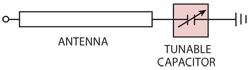
Figure 6 Antenna load tuner.
Applications
Antenna Load Tuning
Today, the load-tuning method described above is being adapted to benefit from higher Q devices with less loss, and also with much greater tuning resolution to fine-tune the frequency selection. Load tuning must be incorporated into the antenna design, as it affects the effective electrical length of the antenna, as shown in Figure 6. The loaded antenna typically has a narrower instantaneous bandwidth and strongly benefits from tuning components with high voltage handling and good linearity.
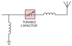
Figure 7 Tunable impedance match (one simple topology shown).
Antenna Impedance Matching
In addition to antenna load tuning, the Tunable Impedance Match (TIM) is enabled by the new tunable RF technologies. As shown in Figure 7, this is basically a reactive tuning network at the input of the antenna (at the 50 Ω interface). If the antenna is not well matched to 50 Ω, the TIM will provide a match over some frequency range. The range of antenna impedances covered with acceptable losses will depend upon the tuner Q and capacitance ratio.
One method of characterizing the effectiveness of an antenna impedance tuner is to look at “Relative Transducer Gain, or RTG.” RTG (or ΔGT) is defined as
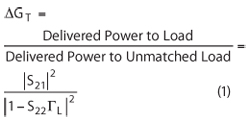
or simply, the power delivered to the antenna with the tuner relative to the power that would be delivered to the same antenna without a tuner. A typical characteristic for RTG is shown in Figure 8 as a function of antenna load magnitude and phase. This figure shows 4 to 5 dB of improvement can be achieved with an antenna exhibiting a 19:1 VSWR.

Figure 8 RTG for a MEMS tuner at 824 MHz.
Other Applications
Tunable Filters
Future uses of High Q tunable capacitors are in tunable filters. These can take the form of notch filters for specific interference rejection (carrier aggregation or simultaneous voice & data applications, for example), or can provide noise rejection for a receive frequency. Requirements for Q, voltage handling and linearity are even greater in filter applications, where voltages and losses are multiplied at resonance. Small step size or resolution is also very important for tunable filters to allow precision control of the filter response.
Power Amplifier Tunable Match
Recent trends in wireless front ends have led to broadband PAs. This allows a reduction in the number of PAs while still supporting the multiple frequency bands required. A switch/filter network is then applied to properly filter the Rx-band noise and harmonics that are generated in the PA. Power Added Efficiency for the broadband PA is reduced as the harmonic frequencies cannot be as effectively terminated. High Q tunable capacitors can be used to provide narrowband matching, with inherent Rx-band noise rejection, and potentially optimized harmonic tuning/filtering. The narrowband match, combined with these other features, can enable very high efficiency PAs, stable and tunable over a wide frequency range, and equally so from CMOS as well as GaAs.
Conclusion
Tunable RF technologies are enabling new frontiers for wireless system RF front ends. The opportunity for smaller form-factor antennas, compensation for head- and hand-loading, and more aggressive antenna designs with higher VSWR over a broader frequency range is allowing for much more flexibility in the industrial design of the handset or tablet. As additional tunable components become available, we will see further reduction in the area and cost of the RF front end along with better RF performance and even wider frequency ranges. The projected performance of tunable RF components will eventually enable “RF Nirvana,” the true software defined radio, where both digital and analog portions of the radio are fully programmable.
References
- “Frequency-Tunable Internal Antenna for Mobile Phones,” 12th International Symposium on Antennas (JINA 2002), Nice, France, November 12-14, 2002, Vol. 2, pp. 53-56.
- “WiSpry Wins First-Ever RF-MEMS Mass-Production Handset Deal,” www.reuters.com/article/2012/01/10/idUS202199+10-Jan-2012+BW20120110.